


China’s Domestic DUV Lithography Breakthrough: Challenging ASML
Short Summary
China’s Ministry of Industry and Information Technology (MIIT) recently added a domestically produced ArF lithography machine to its catalog of state-backed technical equipment. Developed by Shanghai Micro Electronics Equipment (SMEE) and national research institutes, the system represents China’s first major success in building deep ultraviolet (DUV) semiconductor manufacturing equipment capable of addressing sub-28nm process nodes natively, with the theoretical potential to reach 8-nanometer equivalents through multiple patterning.
The announcement highlights Beijing’s intense drive toward technological self-reliance following restrictive export controls from the United States and the Netherlands. While this new Chinese lithography machine currently trails industry leader ASML in throughput and overlay accuracy, its deployment provides a vital lifeline to domestic foundries like SMIC and Hua Hong, reshaping the global semiconductor supply chain and the geopolitical landscape of chip fabrication.
Featured Snippet
China’s domestic DUV lithography machine is a state-developed semiconductor fabrication tool capable of a ≤65nm resolution and ≤8nm overlay accuracy. Built primarily by SMEE, it allows Chinese chipmakers to produce mature node chips independently of foreign technology, with the theoretical potential to reach 8nm processes using multiple patterning techniques.
Introduction
For decades, the global semiconductor manufacturing industry has relied on a highly consolidated supply chain, with Netherlands-based ASML maintaining a near-monopoly on advanced lithography equipment. However, tightened US-led export restrictions have forced China into a corner, sparking a massive state-funded effort to develop an indigenous semiconductor ecosystem.
That effort is beginning to bear fruit. The recent inclusion of a domestically engineered ArF (Argon Fluoride) immersion DUV scanner in China’s official equipment catalog confirms that Chinese manufacturers, led by Shanghai Micro Electronics Equipment (SMEE), have achieved a functional deep ultraviolet lithography tool. While industry experts caution against equating this milestone with the bleeding-edge capabilities of ASML or the extreme ultraviolet (EUV) tools required for the world’s most advanced chips, the deployment of a homegrown DUV scanner drastically alters the strategic calculus of global chipmaking.
Main Article
Understanding DUV Lithography and Immersion Technology
Lithography is the photographic process used to print microscopic circuit patterns onto silicon wafers. Deep Ultraviolet (DUV) lithography utilizes light wavelengths of 248nm (KrF) or 193nm (ArF). The most advanced form of this technology, Immersion DUV (ArFi), places a layer of highly purified water between the scanner’s lens and the wafer. The water acts as a refractive lens, effectively increasing the numerical aperture (NA) and allowing the laser to carve much finer, denser transistor patterns than “dry” lithography.
DUV vs. EUV: The Technological Divide
While DUV handles the bulk of global semiconductor manufacturing, Extreme Ultraviolet (EUV) lithography operates at a 13.5nm wavelength, allowing it to print the extraordinarily small features required for 5nm, 3nm, and 2nm chips in a single pass. EUV tools are exclusively manufactured by ASML, cost upwards of $200 million, and are completely embargoed from shipment to China. DUV systems, while older, can still achieve advanced nodes (like 7nm or 8nm) by using a complex, time-consuming process called “multiple patterning”—exposing the same wafer layer several times to shrink the pitch.
The Drive for Domestic Lithography
China’s push for semiconductor self-sufficiency is a direct response to geopolitics. US export controls, implemented over the past five years and recently expanded alongside the Dutch government, have explicitly targeted China’s access to ASML’s mid-to-high-end immersion DUV systems (such as the NXT:1980Di and NXT:2000i). Stripped of the ability to import the machines necessary for modern chip fabrication, Beijing poured billions into domestic entities to close the gap.
Key Players in China’s Supply Chain
The development of the Chinese lithography machine is a highly collaborative, state-sponsored endeavor.
- SMEE (Shanghai Micro Electronics Equipment): The primary integrator and manufacturer of the scanner.
- AMEC (Advanced Micro-Fabrication Equipment Inc.): A key contributor in etching and associated process steps.
- Chinese Academy of Sciences (CAS): Tasked with solving core optical and photonics engineering challenges.
Current Manufacturing Capabilities and Supported Nodes
The MIIT catalog details a machine utilizing a 300mm wafer diameter and a 193nm ArF light source, with a listed resolution of ≤65nm and an overlay accuracy of ≤8nm. In practical terms, a 65nm native resolution points to the efficient production of 28nm chips via standard single exposure. However, by leveraging aggressive multiple patterning techniques—a method already utilized by Chinese foundry SMIC—this tool is theoretically capable of fabricating chips down to 8-nanometer equivalents.
Technical Limitations
Despite the breakthrough, significant technical hurdles remain. An overlay accuracy of 8nm is substantially less precise than ASML’s leading DUV machines, which boast an overlay of under 1.5nm. Poor overlay accuracy directly impacts manufacturing yield, especially when using multiple patterning. Every additional pattern step introduces the risk of misalignment; at 8nm overlay, the defect rate for advanced nodes will be incredibly high, making mass production of 7nm or 8nm chips on this machine economically inefficient compared to Western standards. Additionally, the throughput (wafers processed per hour) is expected to trail far behind ASML’s 275+ wph benchmark.
Global Industry Reactions
The semiconductor industry has reacted with a mix of validation and skepticism. TrendForce experts have cautioned against interpreting the “8nm capability” as a sign that China has reached parity with TSMC’s 8nm node, noting the vast difference between theoretical capability and high-yield, commercial mass production. However, industry analysts universally agree that achieving a fully domestic tool—bypassing American, Japanese, and Dutch IP—is a monumental engineering feat.
Impact on the Titans: ASML, TSMC, Samsung, and Intel
- ASML: While the Dutch giant will not lose its cutting-edge customers, the rise of a domestic alternative in China threatens its revenue in the mature node market. China previously accounted for over 40% of ASML’s system sales during peak buying periods.
- TSMC, Samsung, and Intel: These bleeding-edge foundries are unlikely to be directly impacted by SMEE’s current generation of tools. However, China’s ability to flood the market with domestic mature-node chips (28nm and above) could compress margins for legacy nodes operated by TSMC and Samsung in the future.
- SMIC: For China’s leading foundry, this is a lifeline. SMIC can now theoretically expand its mature node capacity indefinitely, immune to future US sanctions.
AI Chips and the Supply Chain
The production of advanced AI accelerators (like Nvidia’s H100) relies heavily on 5nm and 3nm EUV nodes, which this domestic DUV scanner cannot support. Therefore, China will still face significant bottlenecks in producing world-class data center AI chips natively.
Future Roadmap: Opportunities and Risks
The primary opportunity for China is absolute security in the mature semiconductor market—chips used in automotive, IoT, and consumer appliances. The risk lies in the “yield trap.” If domestic machines cannot improve their overlay accuracy and throughput, Chinese foundries will be forced to operate at a permanent economic disadvantage, subsidizing low yields through state funding rather than market competitiveness.
Comparison Table: ASML Immersion DUV vs. China Domestic DUV
| Feature | ASML Immersion DUV (e.g., NXT:2000i) | China Domestic DUV (SMEE / MIIT Catalog) |
|---|---|---|
| Country | Netherlands | China |
| Manufacturer | ASML | SMEE & State Institutes |
| Maximum Process Node | 7nm / 5nm (with multi-patterning) | 28nm (native) / ~8nm (multi-patterning) |
| Productivity | > 275 Wafers Per Hour (WPH) | Undisclosed (Estimated low) |
| Overlay Accuracy | ≤ 1.5 nm | ≤ 8.0 nm |
| Availability | High (Global) | Early Phase (Domestic Only) |
| Export Restrictions | Restricted to China by US/Dutch rules | None (Domestic product) |
| Estimated Price | $60M – $80M USD | Undisclosed / Subsidized |
| Target Customers | TSMC, Samsung, Intel, Micron | SMIC, Hua Hong, CXMT, YMTC |
Timeline of China’s Lithography Development
- 2018: SMEE undergoes management changes and secures funding from state-backed investors like China Everbright to accelerate lithography R&D.
- 2020: The US implements sweeping export controls on Huawei and restricts early semiconductor equipment.
- 2022: The US CHIPS Act passes; sweeping sanctions ban the export of advanced AI chips and the equipment to make them to China.
- 2023: ASML faces pressure from the Dutch government to revoke export licenses for mid-to-high-end immersion DUV systems (NXT:1980Di and above).
- 2024: Rumors circulate regarding SMIC manufacturing a 7nm equivalent chip for Huawei smartphones using heavily modified, stockpiled ASML DUV gear.
- 2025/2026: China’s MIIT officially lists the first state-certified domestic ArF DUV scanner with ≤65nm resolution and ≤8nm overlay, confirming indigenous manufacturing capabilities.
Expert Analysis
How significant is this development? According to semiconductor equipment analysts, it is a critical defensive victory for Beijing, but not an immediate threat to the global technological order.
The achievement of a 193nm ArF system with 8nm overlay is roughly equivalent to where Western lithography was in the late 2000s or early 2010s. From a commercial standpoint, attempting to manufacture 8nm or 7nm logic chips on a machine with an 8nm overlay error margin will result in devastatingly low yields. Without EUV, China cannot build the next generation of highly efficient mobile SoCs or data center GPUs natively.
However, from a geopolitical standpoint, it is a masterstroke. The vast majority of chips used in automobiles, military hardware, home appliances, and power management run on 28nm to 90nm nodes. By securing its own supply of lithography equipment capable of servicing these mature nodes, China effectively immunizes the backbone of its tech manufacturing economy against Western sanctions.
Industry Impact
- Chipmakers: Foundries like SMIC and Hua Hong will aggressively adopt these machines to scale mature-node capacity. International competitors like UMC and GlobalFoundries may face intense price competition in legacy nodes.
- Cloud & AI Industry: Cloud providers will not benefit directly, as these machines cannot reliably produce the sub-5nm chips required for frontier AI model training.
- Automotive: A massive win for China’s booming EV sector. Cars rely heavily on 28nm and 45nm analog and logic chips, which can now be fully sourced and manufactured domestically without fear of supply chain disruption.
- Consumer Electronics: Standard consumer electronics (IoT devices, smart home appliances, basic wearables) will likely see a flood of cheap, domestically produced Chinese silicon.
- Global Trade: The “bifurcation” of the semiconductor supply chain is now a physical reality. We are entering an era of two parallel tech ecosystems: one led by the US/Europe/Taiwan, and another entirely contained within China.
Conclusion
China’s introduction of a domestic DUV immersion lithography machine is a watershed moment in the modern tech cold war. While it does not dethrone ASML nor grant China the ability to print cutting-edge AI accelerators, it shatters the illusion that export controls can permanently freeze a nation’s technological progress. SMEE and its partners have successfully navigated one of the most complex engineering challenges in human history. Moving forward, the true test will be whether China can iterate on this foundational scanner to improve yield, boost throughput, and eventually close the gap on next-generation lithography.
FAQ
1. What is a DUV lithography machine?
Deep Ultraviolet (DUV) lithography is a technology used in semiconductor manufacturing. It uses lasers (usually at a 193nm wavelength) to project microscopic circuit patterns through a highly complex optical lens system onto a silicon wafer covered in light-sensitive photoresist.
2. How does Immersion DUV differ from dry DUV?
Immersion DUV places a thin layer of highly purified water between the scanner lens and the wafer. Water refracts light differently than air, effectively increasing the numerical aperture (focusing power) of the lens, allowing for the printing of smaller, denser chip features.
3. What is the difference between DUV and EUV?
DUV uses light at 193nm or 248nm and is standard for mature chip nodes (28nm and larger). EUV (Extreme Ultraviolet) uses a much shorter 13.5nm wavelength, which is strictly required to effectively manufacture the world’s most advanced chips (5nm, 3nm, 2nm) without economically unviable multi-patterning steps.
4. Can China’s new machine print 8nm chips?
The machine has an overlay accuracy of ≤8nm and a native resolution of ≤65nm. While it can theoretically produce 8nm-equivalent chips using complex multiple patterning (exposing the wafer several times), the defect rate and costs would be exceptionally high compared to using Western equipment.
5. Why did China build its own lithography machine?
The United States and the Netherlands have imposed strict export controls preventing ASML—the dominant global supplier—from selling advanced DUV and all EUV machines to China, prompting Beijing to heavily fund a domestic alternative to ensure national tech security.
6. Who manufactures the Chinese DUV scanner?
The primary integrator is Shanghai Micro Electronics Equipment (SMEE), with vital contributions from other domestic firms like Advanced Micro-Fabrication Equipment Inc. (AMEC) and various state-run research institutes.
7. Does this make ASML obsolete?
No. ASML remains the undisputed global leader with a monopoly on EUV technology and a massive lead in DUV throughput and overlay accuracy (ASML’s overlay is ≤1.5nm compared to China’s ≤8nm).
8. Will this impact TSMC or Intel?
Not directly at the cutting edge. TSMC and Intel rely on EUV for their advanced products. However, China’s ability to mass-produce legacy chips could compress the profit margins of older nodes operated by global foundries.
9. Can this machine be used to make advanced AI chips?
Currently, no. Advanced AI chips like Nvidia’s H100 or Blackwell architectures require 5nm or 3nm processes, which necessitate EUV lithography.
10. What does overlay accuracy mean?
Overlay accuracy refers to the precision with which a lithography machine can align a new layer of circuitry on top of a previously printed layer. A lower number (e.g., 1.5nm) is better, as misalignment causes the chip to short-circuit or fail.
Image Requirements (Internal Use)
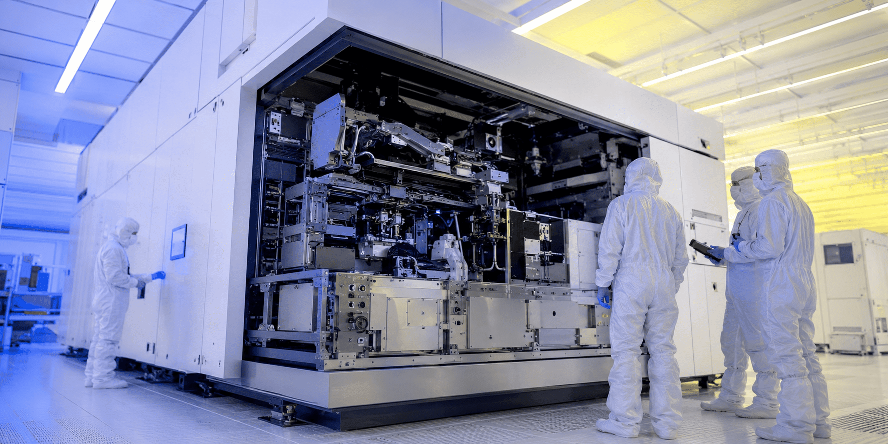
Featured Image Prompt: A hyper-realistic, professional DSLR newsroom photograph of a massive, complex semiconductor lithography machine inside a cleanroom. The machine is sleek, industrial, and highly advanced, surrounded by engineers in full white cleanroom bunny suits. Natural cleanroom lighting with a slight blue and yellow tint. High contrast, sharp focus, 8k resolution, shot on a 35mm lens. No text, no watermarks, authentic Reuters/AP photojournalism style. Ratio 4:2.
- Image Title: China-Domestic-DUV-Lithography-Machine-Cleanroom
- Alt Text: Engineers in a semiconductor cleanroom standing next to a highly advanced domestic DUV lithography machine used for chip fabrication in China.
- Caption: China’s state-backed semiconductor industry has successfully developed a domestic ArF DUV lithography machine, significantly reducing reliance on foreign supply chains.
- Image Description: A professional photograph of a semiconductor fabrication plant cleanroom. Several technicians in white protective suits are working around a large, box-like industrial lithography scanner.
- File Name: china-domestic-duv-lithography-scanner-semiconductor.jpg
Social Media Copy (Internal Use)
X (Twitter)
China just broke through one of the biggest tech blockades in history. 🇨🇳 The MIIT has confirmed the development of a domestic DUV lithography machine capable of printing 28nm natively, with 8nm potential. What does this mean for ASML and the global chip war? Read our deep dive: [Link] #Semiconductors #TechNews #China #ASML #DUV
Major Industry Shift: China has officially entered the deep ultraviolet (DUV) lithography market with a homegrown immersion scanner. Developed by SMEE, the machine boasts a ≤65nm resolution and ≤8nm overlay.
While it currently trails ASML’s bleeding-edge equipment in yield and throughput, this milestone gives Chinese foundries like SMIC a permanent lifeline for mature-node automotive and IoT chip production, fundamentally shifting the geopolitical leverage of US export controls.
Read my full analysis on TechRadar360 covering the technical specs, the yield challenges of multiple patterning, and the impact on the global supply chain. [Link]
The global tech war just hit a massive turning point. China has officially built its own DUV lithography machine to manufacture microchips—a technology previously dominated almost entirely by the West. While it won’t be making the chips for the next iPhone or AI supercomputer just yet, it completely secures China’s ability to produce the millions of chips needed for EVs, smart homes, and defense. Find out how this impacts the global economy and what’s next for the semiconductor industry: [Link]
Hello There. I found your weblog the usage of msn. That is a very
neatly written article. I will be sure to bookmark it and come back to learn more of your helpful info.
Thank you for the post. I will certainly comeback.
Thanks in favor of sharing such a fastidious thought,
piece of writing is pleasant, thats why
i have read it fully